2 PROTOTYPES + APPLICATIONS
The following chapter reviews
potential applications, and the various demonstrator products which have
been constructed.
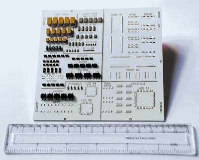
The majority of the prototypes have used an epoxy based conductive
adhesive (RS Part No. 496 265) for component attachment. This has proved
well suited to the purpose. Trials with industry standard pick and place
machines at Mitel Telecom have confirmed the suitability of this
technology for high-speed component population of lithographic films.
Substrate choice is a major contributing factor to the cost and
successful implementation of this technology. Coated, cellulose based
(GlossArt) papers, and polyethylene based synthetic papers have been
widely employed. About 30 different substrates have been trialed,
including Industry Standard FR4 and materials such as polyimide (Kapton
®) and polyester (Melinex ®).
2.2.1 Microwave patch antennae
Following investigation of the characteristics of printed microwave
striplines, a manufacturer of microwave frequency systems expressed
interest in the process as mechanism for reducing manufacture costs. The
company was particularly interested in patch antennae, devices which are
currently fabricated from etched ‘FR4’. These capacitively coupled
to the transmitting and receiving circuitry, avoiding electrical or
soldered connections. The price of each antenna unit was approximately
15 pence and the primary driver was to reduce the cost.
A series of printing trials on ‘GlossArt’ and ‘PolyArt’ were
used to determine the dielectric characteristics of the substrates at
particular thicknesses using a parallel-plate capacitor model. These
values were employed to generate substrate specific patch antenna
artwork, designed to resonate at particular frequencies. In addition,
the feed line to each patch was increased in thickness to compensate for
the higher resistance of the printed films. The printed samples were
evaluated using a microwave network analyser to determine actual
resonant frequencies, and assembled into otherwise unmodified products
to determine the functional performance against unmodified devices. The
resonant frequencies of the two substrates varied from the ‘FR4’
sample by 4% and 13%, indicating the devices were not optimised for the
resonant system they were to be included in. Measurements of the
performance of the assembled devices resulted in reduction in
performance, (compared to etched copper), of 40% and 75% respectively.
These superficially disappointing results were attributed to mismatch
loss and gain loss of the antennas not being resonant at the test
frequency.
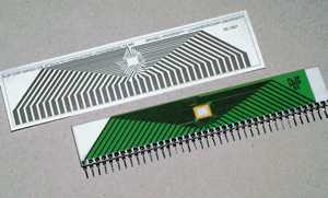
A lithographically printed (left)
and a conventionally
manufactured (right) Patch Antenna.
2.2.2 Flip Chip
‘Flip-Chip’ is a process of attaching integrated circuits
directly to a circuit board substrate, instead of utilising standard DIL
and SMT packaging. This is achieved by the following process: The bare
silicon chip is bumped, a process of creating raised areas where
connection to the board is required. The chip is then turned and placed
face down, ‘flipped’ on the substrate. To ensure electrical contact
between the silicon and the substrate a variety of adhesives are used.
For many applications, where the small size of the connections to be
made prohibit the use of mechanical devices or standard conductive
adhesives. Anisotropic adhesives offer the potential of good electrical
connectivity and mechanical strength. Dr Samjit Mannan (Loughborough
University) undertook an initial study of the suitability of conductive
lithographically printed films for use as substrates for flip-chip
assemblies using two anisotropic conductive adhesives.
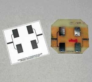
Two test patterns were replicated from existing alumina tiles and
printed, samples of ‘GlossArt’ and ‘PolyArt’ substrates were
supplied to Loughborough for assembly. Whilst temperature stability of
the polymer substrates was a problem, two of the three paper samples
offered 100% connection of all joints, and the other 62.5%.
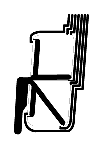
Flip-Chip adhesion and joint test
structures.
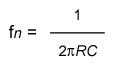
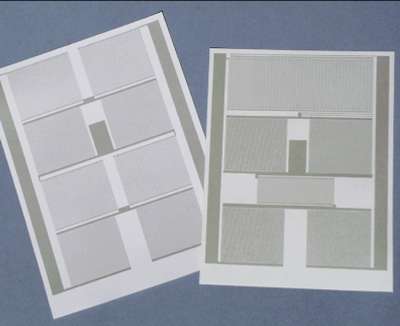
2.2.3 Printed Passive Filter
Networks
Passive RC notch filter networks absorb a narrow band of frequencies
whilst transmitting all others. The lithographic printing of conductive
inks enables the fabrication of such devices from a single ink and
plate. The ‘Twin T’ filter developed relies on critical matching of
the component values to deliver a sharp notch at a frequency given by
the rule:
The convoluted printed component
structures had design resistances of 20kOhm and capacitances of 100pF.
The interwoven resistor structures reduced relative variation in
resistance to ±1% and ±10% absolute tolerances throughout the print
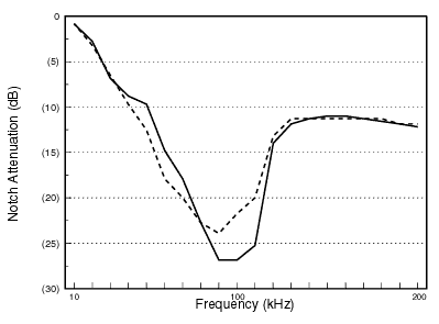
run. Upon application of a swept frequency sinusoidal signal to the
input of the device notch attenuations of ~25 dB were recorded at ~90
kHz, with notch bandwidths of ~30 kHz. The solid line represents results
of a filter with trimmed resistors, whilst the dashed line represents an
as printed specimen.
'Twin T' printed filter
structures. Note the inter-woven resistor
structures designed to give good relative tolerances, achieved ±1%.
Frequency response curves of two
'Twin T' filter structures,
the solid line represents a closely matched sample.
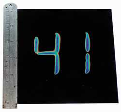
2.2.4 Display Structures
Several prototype reflective display devices have been fabricated
from low cost thermochromic substrates and printed electrode structures.
The possible applications for these types of display range from low-cost
large area devices to inductively heated single shot tags, such as could
be used to verify packaging integrity.
The devices function by heating a localised area of the thermochromic
substrate, the electrode structure for each segment consists of a narrow
track designed to dissipate a specific quantity of energy as heat. For
the network illustrated each element has a dispersion of ~1.3 mW/mm when
run from a 3V supply. If several elements are to be used in a single
display care is needed to match the power dissipation/length of each, to
avoid uneven heating.
Various thermochromic substrates are available, and a suitable colour
change temperature can be selected for the desired environments. The lag
time (the time taken for an electrical change to effect a visual change)
is dependent upon the ambient temperature, thermal conductivity,
specific heat capacity, and the power dissipation of the assembly, and
can range from several seconds upward. Control of the power dissipated
by the elements enables lag times to be reduced to a couple of seconds
by delivering a high power ‘start’ followed by a lower power
‘maintenance’ phase, similar to chokes and starters on fluorescent
tubes and large motors.
Single-sided electrode structure
for a thermographic seven-segment
display. Note the 100 µm width tracks which dissipate ~1.3 mW/mm at 3V.
A large digit reflective
thermochromic/lithographically printed display.
The current drawn by each segment was ~20 mA, similar to a standard LED.
2.2.5 Polymer Light Emitting
Devices
Light Emitting Polymer structures utilising optimised inks are under
investigation in a joint Brunel University/Durham University EPSRC
funded project (Project No. GRM01982). The Durham team is lead by Dr
Ifor Samuel. There is currently great interest in the use of conjugated
polymers to make light-emitting displays following the discovery of
polymer electro-luminescence.
Polymer light-emitting diodes (LEDs) offer the prospect of colour
light-emitting displays that are flat, operate at low voltage and are
even compatible with flexible substrates. These devices typically
consist of one or more polymer layers of total thickness approximately
100 nm in between two contacts. When a voltage is applied, the polymer
emits light. To date the contacts have generally been deposited by
thermal evaporation or sputtering. We have examined the feasibility of
using offset-lithography to deposit contacts for polymer LEDs.
Lithographic printing is faster than evaporation or sputtering, and
could lead to the much-improved manufacturability of polymer displays.
CLF Light emitting diodes were fabricated by spin coating a solution of
MEH-PPV (more fully known as poly(2-methoxy,
5-(2’-ethyl-hexoxy)-1,4-phenylene-vinylene) from a chloro-benzene
solution onto a CLF printed track. The concentration of the solution
determined the polymer layer thickness. The top electrode, a 30 nm
aluminium layer, was thermal evaporated at a pressure of 0.000001 mbar
The thin top contact layer thickness was necessary to allow light to
pass through. Testing of the devices was performed under vacuum and for
all results reported the CLF was wired as the anode.
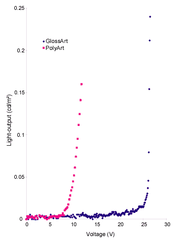
The current-voltage characteristics are nonlinear and are typical
characteristics for polymer LEDs, apart from a relatively high turn on
field due to the large device thickness of typically 260 nm, and large
barrier to charge injection from the contacts used. We have successfully
demonstrated that polymer light-emitting diodes can be fabricated with
silver-based conductive lithographic film printed contacts. These
results represent a significant step in the low-cost manufacture of
flexible light-emitting displays.
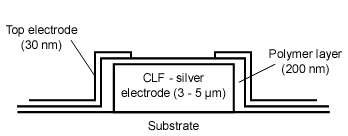
Schematic of CLF/LED
Voltage - light output
characteristics for polymer light-emitting
devices made from GlossArt and PolyArt.
2.2.6 Printed Capacitors
A key area of research interest is the fabrication of capacitor
devices using the CLF process. The aim of this work is to develop a
strategy for manufacturing small capacitance value (<10nF) components
as integral parts of the circuit’s substrate. Printed capacitors could
be suitable for roles such as coupling, decoupling, timing networks and
sensor applications.
A number of approaches to electrode capacitor manufacture have been
explored including the printing of interdigitated structures, dielectric
ink films and the use of plastic film dielectrics. Interdigitated
capacitors are structures comprising two ‘comb-like’ electrodes
separated by a fixed gap. The components are printed onto the surface of
the substrate with standard conductive ink and can form an integral part
of circuit interconnect. The capacitance of the structures is largely
due to the fringing field passing through the substrate between the two
electrodes. The components are typically low in Capacitance value per
area (<15pF/cm2) but are useful in applications where low-cost
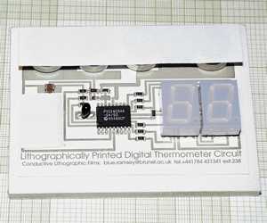
non-critical devices may be specified. The picture above shows an
unpopulated thermometer circuit that uses a printed capacitor in an RC
network and printed pull-up resistors. Multilayer Capacitors have been
constructed by sequentially printing conductive and dielectric ink
films. This work required the formulation of suitable dielectric inks
containing high proportions of titanium dioxide (rutile). The
formulation of the inks was completed in collaboration with Gwent
Electronic Materials (GEM). These inks were designed to offer high bulk
dielectric properties, and exhibit shear-thinning characteristics
necessary for offset lithographic printing. The relative bulk dielectric
constant of the ink is ~14. Devices have been fabricated by printing a
3-5µm conductive film and overprinting with successive layers of
dielectric ink to achieve a layer of ~20µm. A conductive layer was then
printed onto the dielectric layer to form a multilayer capacitor
structure. Capacitors manufactured in this fashion offer Capacitance
Densities of ~650pF/cm2.
Recent efforts have focused on possible solutions for embedding
capacitors within plastic substrates. Multilayer circuits containing
capacitors can be built up with the use of thin polyester films.
Capacitor structures and interconnect can be buried within a flexible
substrate by printing conductive films and laminating over them with the
plastic film. The various layers of the structure can be connected with
drilled holes and printed vias. Devices manufactured in this fashion
offer capacitance densities of ~110pF/cm2 for a single dielectric layer.
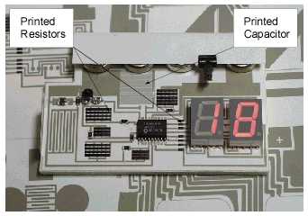
Printed Thermometer Circuit with
Interdigitated Capacitor
2.2.7 Surface-mount-technology
component attachment
For CLFs to be fully integrated into a high-volume production process
the adhesion characteristics of a range of surface-mount-technology (SMT)
component packages and conductive adhesives were evaluated. A standard
alumina tile employed in solder-bond shear strength measurements by
Mitel Telecom was employed. Patterns were printed onto PolyArt and
Teslin substrates which were then adhered to the alumina tile blanks to
allow automatic handling, including adhesive dispensing, auto-placement
of SMT components and adhesive curing.
The tile-mounted CLFs were populated in a similar manner to the standard
alumina substrates. Each tile was screen printed with a specially chosen
conductive adhesive, and populated with a range of solder-tinned SMT
packages using a pick-and-place machine. The component bonds were
thermally cured by a temperature profile matching the cure
characteristics of the adhesive.
Analysis of the bond failure mechanisms have demonstrated that bond
strengths of between 30% to 50% of the strength of soldered joints on
sintered silver-palladium thick film conductors have been achieved. This
is in agreement with adhesive bond strengths recorded by the
manufacturer, involving similar SMT components and conventional circuit
board substrate materials.
A populated CLF substrate.
2.3.1 Statesman Telephone handset
To demonstrate the capacity of the printed films to form complex
electronic interconnect, telephony circuitry was selected. Modern
telephones contain a network of analogue and digital sub-systems
operating at moderate currents and potentials approaching 50V.
The fabrication route adopted was to replicate a ‘Statesman’ (circa
early 80’s British Telecom) telephone circuit. Circuit artwork was
generated by desoldering and scanning an existing Statesman circuit
board. The scanned artwork required substantial reworking to remove all
the unwanted soldermask and component labelling. The image was
transformed into 2-bit black and white, and the circuit tracks thickened
wherever possible to accommodate the higher sheet resistivities of the
printed film. The completed artwork was printed onto ‘GlossArt’ and
‘PolyArt’ substrates. The original circuit board from the telephone
was stripped of the soldermask permitting the copper tracking to be
etched off. The printed film circuitry was laminated to the bare board
to provide the printed substrate with mechanical integrity. The 64
through-hole components, including two ICs, were attached with a
conductive electrical touch-up paint (RS Part No. 186 3600) to the
circuit board pads. The fully assembled and functional circuit was
replaced in the original casing. The unit was tested for faults and load
impedance on a British Telecom line simulator (Silicon Arrays Part No.
Telecom Tester Type T-073), and used extensively on the internal
university network.
The electronic success of this demonstrator proved unequivocally the
ability of the process to form complex functional analogue circuits, and
illustrated the possibilities of the process for switchpadapplications.
Unmodified and modified
'Statesman' telephone circuitry (not to scale).
2.3.2 Microprocessor Thermometer
The thermometer consisted of a PIC microcontroller and associated
circuitry, zinc/air cells and low power seven segment displays. The
microcontroller used an external RC combination to set the speed of the
processor to 4 MHz, and the temperature was calculated from the time
taken to discharge a capacitor through a thermistor.
Several of these devices have been constructed and have proved very
reliable. The substrate is used to form not only the electrical
interconnect but the cell holder and switch for the device. Versions
have been constructed on ‘GlossArt’, ‘Teslin’, polyester and
‘FR4’ substrates. The first of these demonstrators has now been
operational for 2 years. The assembled circuits were not lacquered or
otherwise protected, and though discolouration of the tracks has
occurred the function of the devices has not been impaired.
Microprocessor thermometer,
designed to illustrate the surface-mount
and digital applications of this technology.
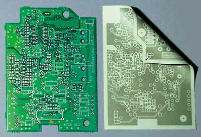
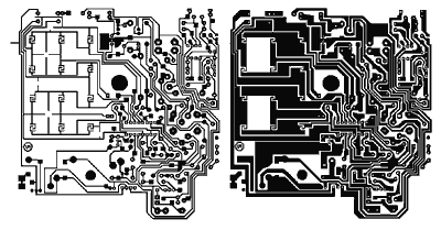
Conventional and Lithographically
printed circuit boards for telephone assembly.
This demonstrator surpassed all others in complexity and processor
speed.
2.3.3 Nortel Telephone handset
To demonstrate that lithographically printed films may be used
successfully in complex mixed signal, double sided, surface mount
circuits; a modern, fully featured telephone circuit was fabricated.
Nortel provided three sample C8009 telephones, circuitry artwork and
components.
The printed circuit board assembly comprised through-hole and
surface-mount devices soldered to 1.6 mm ‘FR4’ laminated with 35µm
copper. Plate artwork was prepared and printed with care to ensure
accurate alignment of the two sides. Two versions, one with thickened
tracks, were printed though ultimately this proved unnecessary as the
unmodified circuitry was used and proved satisfactory. Assembly of the
prototypes required manual drilling of the ‘PolyArt’ substrate to
create via holes which were filled with conductive adhesive to achieve
electrical continuity. The 133 components were attached in order of
decreasing complexity, and checked for short or open connections, as no
solder or adhesive mask was used.
The assembled board was tested in the same manner as the ‘Statesman’
before being connected to the university network. Successful operation
was achieved, with crisp and clear audio.
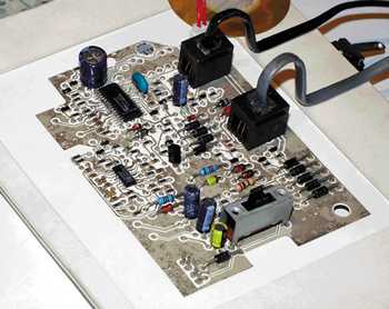
Assembled circuit, illustrating
the complexity and scale of the device.
The keypad attached to the underside of the circuit was largely
unpopulated.
The large black sockets connect the line in, and handset to the circuit
and
the piezoelectric ringer is partially visible top of the photograph
|