PAPER MEMBRANE SWITCHES FOR FULLY
FEATURED COMPUTER KEYBOARDS
This case study documents the
successful development and evaluation of a novel membrane switch. The
process results in lower environmental burdens and manufacturing costs
than current screen-printed polyester solutions. Parameters governing
the successful application of new materials to switchpad circuits
include track resistance, migration resistance and switch contact
resistances.
These have been characterised and are reported. Lifetime tests have been
conducted and the printed films exposed to a regime of standard 85RH/85
°C and corrosive atmosphere tests. The lifetime of the switches has
been investigated, and exceeds the normal industry specification.
Several fully featured demonstration keyboards and switch membranes have
been constructed and tested. These are currently in use in office
environments.
In 1999 112 million computers were
produced. The requirement for cost effective manufacture in this area is
intense. Early keyboards were constructed of individual mechanical
switches, but these suffered from short service life. Industry required
lower cost higher reliability solutions. The systems developed to fill
these requirements fall into two broad categories, Membrane and Pad
switches.
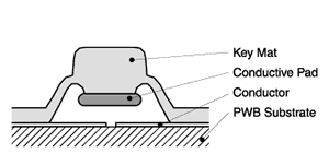
Pad switches typically utilise a printed circuit board within the
product to carry the conductive traces and to provide mechanical support
as the switch is pressed. Both switch contacts are formed on the
substrate as part of the etched circuit pattern and protected by a
chemically stable, conductive coating such as gold or carbon paste, to
prevent corrosion. The switch is activated by pushing a conductive pad
onto both contacts, enabling electrical conduction.
Simplified diagram of a pad
switch.
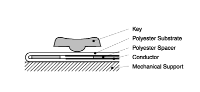
Larger, more complex keyboards and
switch arrays usually utilise membrane switches. These typically consist
of a polyester substrate screen-printed with silver paste to form the
conductive traces and switch contacts. The substrate is folded back on
itself, or faced to another printed sheet, and the conductive traces
separated by an insulating spacer. The spacer is typically a polyester
sheet with holes punched where the switch contacts need to touch, but
may be a thick screen-printed dielectric layer. Activation of the switch
is achieved by ressing the two contacts together.
The electrical characteristic of most importance to membrane switch
operation is electrical resistance can be considered to comprise two
elements, the line resistance and the contact resistance.
Simplified diagram of a membrane
switch.
Line resistance is the total
resistance of the printed track, leading to and away from the switch
contacts. It is determined by the bulk resistivity of the printed ink
and the physical geometry of the circuit track. The industry usually
simplifies this further by using sheet resistivity (Ohms per square)
figures, which assume a constant film thickness and allow easy
calculations of line resistance if the length and width are known.
Contact resistance is somewhat more variable, and is influenced by the
switch closing pressure, switch contact geometry, switch contact
corrosion and contact topography.
Switch closing pressure is primarily determined by the force with which
the key is depressed, but is also influenced by the pad design and the
area of contact the key has with the top membrane. Corrosion products on
the contacting surfaces will have a detrimental effect on contact
resistance. For most domestic and office environments barrier coatings
are not necessary. Contact topography is largely determined by the ink
paste and deposition process, though it will change over the switch
life. Typically, the root mean square (RMS) roughness of the printed
switch contacts will be several microns (10 -6 m). Rough contacts have
higher resistances than smooth counterparts, as the points of contact
are fewer. Contact resistance normally increases as the switch is
repeatedly used; an increase of 20% over 20 million cycles is not
untypical.
The service life required of a membrane switch is dependent on the
application it is used for;
|
Application
|
Life Cycles
|
|
Computer Keyboards
|
2.00 E 7
|
|
Typewriters
|
1.00 E 7
|
|
Copiers & Telephones
|
1.00 E 6
|
|
Calculators
|
5.00 E 5
|
|
Toys & Games
|
1.00 E 5
|
Typical switch life requirements
The likely cause of failure of a
membrane switch is usually either electrical or mechanical wear of the
switch contact surfaces, or chemical corrosion. Mechanical wear of the
contact surfaces will occur if the switch contact fragments due to
repeated compressive loading. Excessive electrical wear will result if
the switched current is too high. Every switch cycle comprises an
instant where the electrical current will pass through an infinitely
small contact point. As this occurs the heat energy build up from the
increased contact resistance can be enough to erode the contact. This
may result in lost contact material, or a movement of material from one
contact to the other.
Corrosion products can cause failure by two mechanisms, contact
insulation and migration. Contact insulation can occur if elements of
the ink film react with atmospheric pollutants. Sulphurous gasses can be
particularly problematic, though the level found in most modern
environments is generally insufficient to cause problems. Careful design
of membrane and track geometries has also been employed to reduce
exposure. Migration occurs if a potential gradient and critical
quantities of moisture occur between two silver loaded circuit tracks.
It is an electrochemical reaction resulting in the growth of conductive
silver dendrites between the tracks, eventually resulting in a short
circuit. Careful circuit design, minimising steep potential gradients in
the same plane, minimises dendrite formation. The voltage and current a
keyboard membrane switch operates at is determined by the circuitry it
is in electrical contact with. In most cases this is an encoder IC. The
encoder determines which switch on the matrix has been closed and sends
the appropriate serial data to the CPU. Encoders present very high
impedance to the membrane circuitry. This ensures only minute current
flow occurs when the switch contacts are closed, and enables the use of
moderately high resistance membrane circuitry. Typical current flow in
contemporary computer keyboards is normally less than 0.1 mA, and the
potential applied is normally 3-9 volts. The closed switch resistance
permissible may be as high as 10 Kohms, though in practice the combined
printed track and switch contact resistances are seldom higher than 500
Ohms. Open switch resistance needs to remain higher than the maximum
permissible closed switch resistance if the encoder is not to
erroneously trigger. In practice open switch resistances are seldom
lower than tens of MegaOhms unless there are high levels of moisture
present between circuit tracks or migration has occurred.
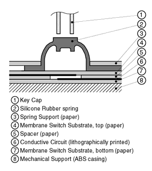
Method
To assess the application of CLF circuitry printed on paper for keyboard
membrane switches, the screen-printed polyester components of an
existing product were replaced. The Cherry® Business Line® keyboard
was selected as it offers a highly optimised design. A rubber spring
acts as the key return and determines the tactile feedback the keyboard
user experiences. This design enables the mechanical aspects of each key
to comprise just three separate parts, two of which are common to the
whole product; the product housing, and a rubber spring, the third being
each individual key cap. This contrasts to many other designs, which use
individual spring and key cap mountings for each key.
Simplified diagram of the switch
mechanism employed in the Cherry® keyboard.
Both of the Membrane Switch Substrates are formed from a single piece of
material,
which is printed, die cut, and folded over so the printed side contacts
itself
through the holes in the paper spacer.
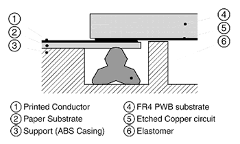
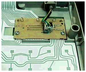
Simplified Membrane Circuit to PWB
Connection. The printed paper circuit
is connected to the encoder PWB by screwing the PWB into place, trapping
the membrane circuitry between the PWB and an elastomer.
The printed paper membranes were
prepared using an identical circuit layout to the screen-printed
originals. The printed track width was 0.6 mm. The substrate chosen was
a standard Gloss Art 80 gsm filled paper, usually used for glossy
brochures and magazines. The substrate was imaged using a Heidelberg
offset lithographic press, though Roland presses have also been
successfully employed. No post printing curing phase was implemented. If
it is considered necessary, the sheet resistivity of the printed films
can be reduced by about 30 percent by hot air curing at 100 °C for 5
minutes.
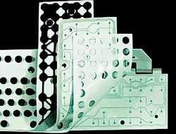
Paper membrane switch constituent
parts, to right:
spring support, switch circuitry, spacer, switch circuitry
Lithographically printed paper
switch membrane.
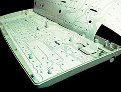
Final assembly of the encoder PWB
and paper switch membrane.
Results
Circuit Track Resistance The sheet resistivity of the paper membrane
switch circuitry is ~ 150 mOhms/sq. This compares to about 75 mOhms/sq.
for the screen-printed original. Resistivity measurements were averaged
measurements obtained using a four-point probe Low OhmMeter. The
resultant track resistances are about twice that of the original, just
over 400 ohms in the worst case. The contact resistance is also about
twice that of the original circuitry. The total switch resistance, worst
case scenario, is ~ 600 ohms, comprising contact resistances of ~ 1 ohm,
dependent upon key pressure.
Migration Resistance There are as yet no international standards
for testing the susceptibility of printed tracks to migration. Initial
work at Brunel indicates migration resistance of the lithographic ink
films and the conventionally manufactured screen-printed films are
comparable.
Lifecycle Performance
The lifecycle performance of membrane switches is normally determined by
placing a unit in a mechanical jig, which activates the switch, whilst
under electrical load, and increments a counter if a closed circuit is
detected. These jigs typically operate at 3 cycles per second and will
tolerate 2 consecutive null returns, i.e. open circuit, before
terminating the test. The contact life of the CLF paper membrane switch
has been tested to 25 million cycles, a figure in excess of most
keyboard specifications, without failure. In addition to the mechanical
lifecycle testing, two keyboards have been in use in real world office
environments. One of these has been in place for 6 months without
failure.
Conclusions
This work has demonstrated the suitability of lithographically printed
paper membrane switches for computer keyboard applications. Acceptable
electrical performance and mechanical longevity has been demonstrated.
Paper/cellulose based substrates can achieve acceptable levels of
reliability for application in contemporary electronic products. Coupled
with the high production speed and low volume /unit ink requirements of
offset lithographic printing this fabrication process can offer
environmental benefits of: Reduced non-renewable resource use, as
polyester is replaced by paper/cellulose material; Lower energy per unit
manufacturing cost; Reduced raw material use as the quantity of
deposited silver conductor is reduced.
|